At long last, chip giant Intel (NASDAQ: INTC) opened up about its upcoming 10-nanometer chip manufacturing technology, at its first-ever Technology and Manufacturing Day. The company has -- frustratingly -- kept key details of this technology under wraps for years now, but Intel is now putting them out there for all to see.
Without further ado, let's look at what Intel had to tell us about this new tech.
A large jump in density
Let's talk performance
Competitive comparison and no yield information
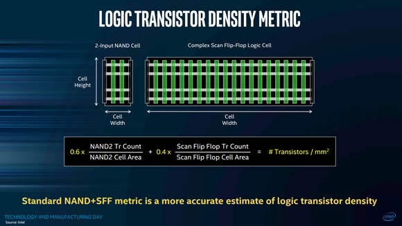
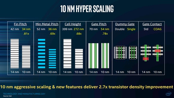
Image source: Intel.
Chipmakers generally like to reduce the area of its transistors with major new technology shifts. This area reduction is important in reducing transistor costs on a yield-normalized basis, a really important factor for product cost. Chipmakers are ultimately able to cram more features and functionality into a chip while maintaining reasonable cost structures.
Intel says that in moving from 14 nanometers to 10, it's delivering an increase in transistor density by a factor of 2.7. Part of that density increase is due to reducing key aspects of the technology, such as the gate pitch, minimum metal pitch, and cell height. (Intel provides a ) of these and other terms.)
Beyond those reductions in feature size, Intel also says other technology advancements in the technology help it further reduce chip area, referring collectively to these techniques as "hyper scaling."
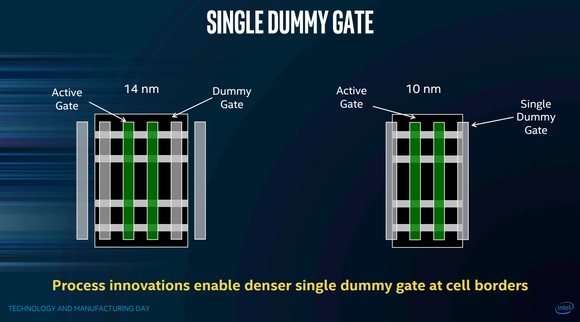
The first advancement, Intel says, is a move from using two dummy gates per logic cell to a single one. A dummy gate, Intel explains, is a "gate that isn't part of a transistor, put on the edge of a logic cell, needed to isolate one cell from another."
The company asserts that moving from using two dummy gates per cell to one drives a roughly 20% reduction in chip area size.
The second advancement is what Intel refers to as "contact over active gate," a "process feature whereby the gate contact is stacked on top of the transistor gate rather than at its side." The net benefit, Intel claims, is a roughly 10% reduction in chip area.
Adding all of this together, Intel says its 10-nanometer technology delivers a 2.7-fold improvement in logic transistor density. Now, not all transistors on a chip are logic transistors -- there are SRAM and I/O, for example -- so Intel is claiming chip-level area scaling of about 0.43, or approximately a 2.33-fold improvement in density, for a "representative" chip that includes logic, SRAM, and I/O.
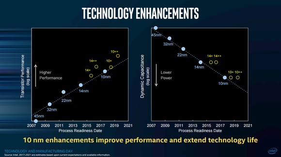
In addition to density, Intel talked about the performance and power consumption of its various manufacturing technologies.
Intel claims that its 10-nanometer technology can deliver either a 25% improvement in performance at a given level of active power consumption -- that is, when the transistor is doing something -- or it can deliver the same performance at 0.55 times the power of its 14-nanometer technology.
What's interesting, though, is that in terms of transistor performance, the picture doesn't look as rosy as the density picture that Intel provided. For instance, Intel says its first-generation 10-nanometer technology delivers only slightly more performance than its current-generation 14-nanometer+ technology, which is used to build Intel's latest PC processors today, and performs worse than the company's 14-nanometer++ technology that will be used to manufacture the company's upcoming eighth-generation Core processors.
Image source: Intel.
Even Intel's second-generation 10-nanometer technology, known as 10-nanometer+, is expected to perform slightly worse than 14-nanometer++. Only by the time Intel gets to its third-generation 10-nanometer technology, 10-nanometer++, will 10-nanometer performance clearly exceed 14-nanometer++ performance.
A silver lining, though: Intel says that all three of its 10-nanometer flavors offer lower dynamic capacitance than all three of its 14-nanometer variants, which the company says translates into lower power consumption.
Intel took the opportunity to compare the density of its 10-nanometer technology with what it thinks the competition will deliver with their respective 10-nanometer technologies.
Intel claims that, using a metric that's essentially the weighted average of the transistor densities of a two-input NAND cell and a complex scan flip-flop logic cell, its 10-nanometer technology is about twice as dense -- or a "full generation ahead" of competing 10-nanometer technologies.
Image source: Intel.
However, one thing I was disappointed by was that Intel is comparing its 10-nanometer technology to competing "10-nanometer" technologies.
The reality is that Intel's 10-nanometer technology will probably have to slog it out with competing "7-nanometer" technologies in the marketplace, so it doesn't seem fair to compare Intel's 10-nanometer tech, which won't go into production until the second half of 2017, with foundry 10-nanometer technologies, which are in production now.
To illustrate my point, Intel's chief competitor, Taiwan Semiconductor Manufacturing Company (NYSE: TSM), has said that its 7-nanometer technology, which should go into mass production in the first half of 2018, delivers a roughly 1.63-fold density improvement over its 10-nanometer technology.
Intel's 10-nanometer technology should be, on an apples-to-apples basis, denser than TSMC's 7-nanometer technology, at least in logic, as TSMC disclosed that its high density 7-nanometer SRAM cell is a bit denser than Intel's. But things seem to get murkier for Intel's logic density leadership position in 2019.
TSMC also says an enhanced version of its 7-nanometer technology, known as 7-nanometer+, will deliver another 15%-20% logic area improvement over its 7-nanometer technology .
A quick calculation suggests that TSMC could be able to close the density gap with Intel's 10-nanometer tech once it gets its 7-nanometer+ technology into high-volume manufacturing. I'd expect TSMC to be cranking these chips out in mass quantities in support of the 2019 iPhone.
And, finally, Intel didn't provide any information on manufacturing yields. That the technology hasn't yet qualified for production, coupled with the fact that Intel is likely to keep the bulk of its processors shipments on 14-nanometer technology in 2017 and probably most, if not all, of 2018, seems to suggest that they're not great.
Comments
Post a Comment